The P10 Display.
In this post, we will be seeing on how can we use the STM8s microcontroller to drive the Chinese dot matrix display. In this process we will be understanding how exactly does the display work (the schematics and work flow), and further will be interfacing the display with the STM8s Discovery Board (both the code and hardware will be discussed.) Once we understand how the display works, writing the code should be a piece of cake then.
What is the P10 display?
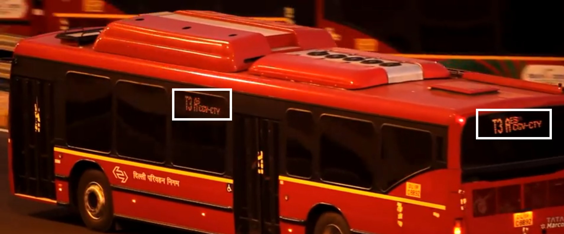
The P10 display is an LED Panel, a very cheap one, 32X16 i.e has 32 LED’s in horizontal and 16 in vertical (one panel). The 10 in P10 stands for the pixel distance that is 10mm. It is widely used in advertising and to grab attention in local markets. You must have seen a variant of P10 display on the Buses in Delhi (image below). This one has a much bigger pixel distance something around 13-15mm so these might be P13 or P15 displays but the working concept is the same. Further, we can cascade more and more LED panels to get a bigger panel.

The thing about these Chinese displays are that they come with absolutely 0 documentation. I tried searching on the web and was able to find a few russian blogs but it did not help much. These displays are based on an undocumented protocol (hub12). The Chinese don’t want anyone to replicate their extreme low cost design and remove their monopoly in this market so they dont provide any reference to understand their products. However, this not being a very complex device, it was easy to reverse engineer the display.
The display
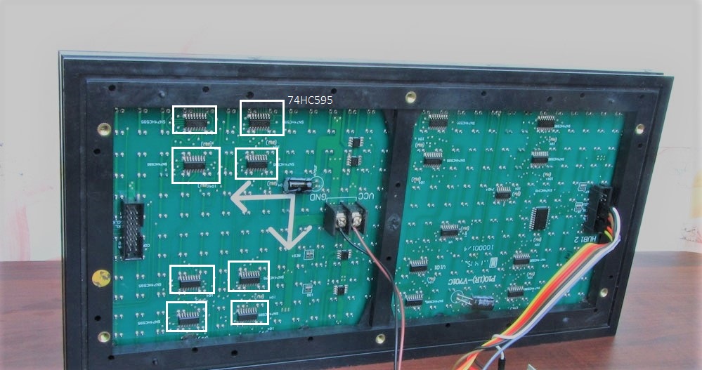
The front panel consists of 512 LED’s in a 32*16 matrix. On seeing the backside of the panel we see sixteen 74HC595. This is an 8 bit serial-in parallel-out Shift Register.

Every single 8 bit shift register can be used to control 8 LED’s. So we can control 128 LED’s by the given number of shift registers on one panel but the number of LED’s are 512. How does the display control 512 LED’s when it is just capable of controlling 128 LED’s? Here comes the concept of refresh rate.
At one instant, the shift registers can only control at a maximum of 128 LED’s so we select which of the 128 LED’s to be controlled by using two extra bits. The rows switch faster than the refresh rate of the human eyes, such that for the human eye it looks static. Think of this as when you take a laser light and move it from one place to another, you see a line of that laser light, but is it actually a light? Its just a dot in real. This is the concept of refresh rate used in this P10 display to smartly reduce the production cost. To understand this concept better, see this image. It took me an hour or two to figure out how data shifts through the 74HC95. I’d recommend the reader to try this on their own after reading this post. Refer the picture on the right.

The white boxes show the LED’s controlled by every shift register. At one instant only one row out of the four can be enabled/controlled by using the A and B control bits as below.
| A | B | Row |
|---|---|---|
| 0 | 0 | 1,5,9,13 |
| 0 | 1 | 2,6,10,14 |
| 1 | 0 | 3,7,11,15 |
| 0 | 0 | 4,8,12,16 |
Now that we know how exactly the display works, we can get started on writing the code and making the hardware connections to display any content on the display. Things will be a lot clear once we write the code and make the connections.
The Connections
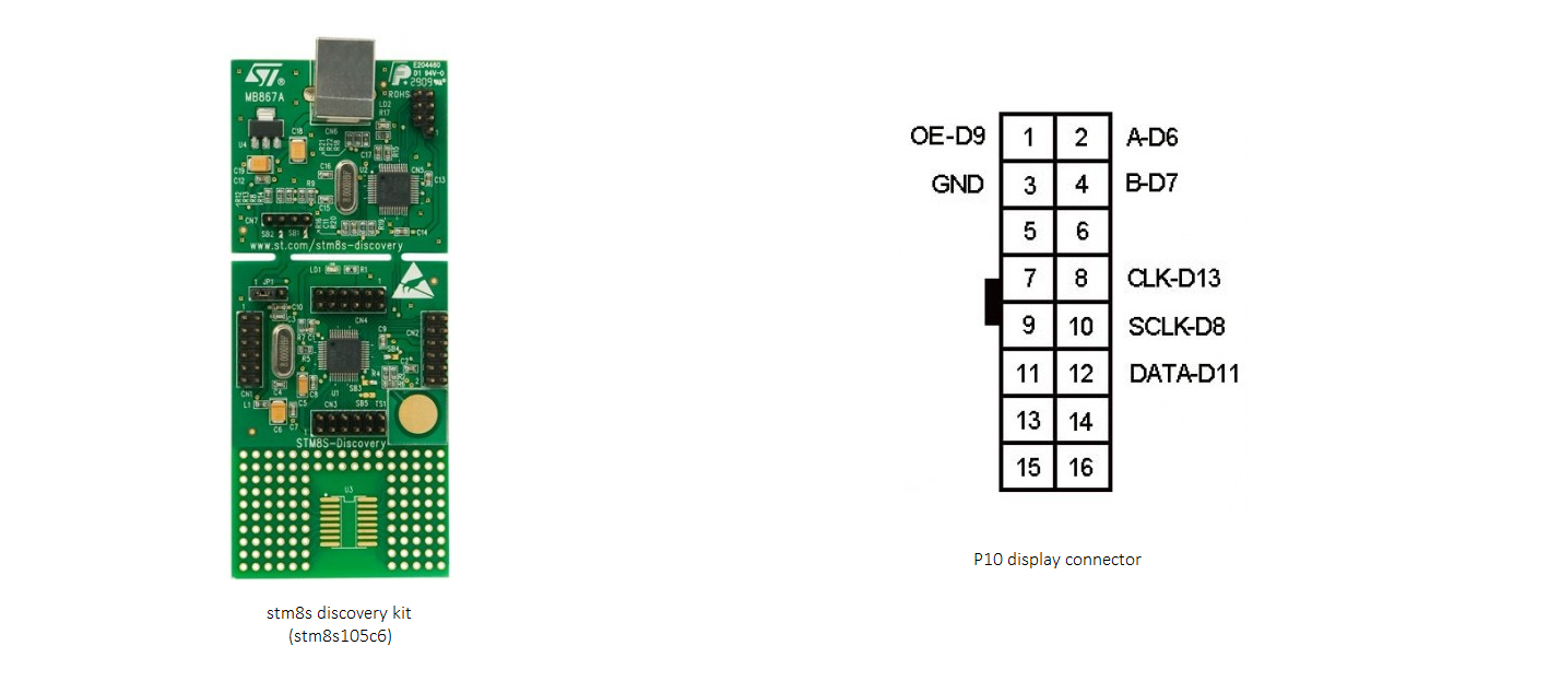
The connections are pretty straight forward. The pin configuration for the display was available online (shown in the image below) , and as we are communicating through SPI, we just need to configure the pins accordingly. Do keep the pin configuration of the STM8s discovery board handy. It is available here.

The connections which I have used are as follows: Refer the user manual to understand these connections.
1  => CN2 3
3  => CN1 5
2  => CN2 11
4  => CN2 5
8  => CN2 6
10 => CN1 9
12 => CN2 9
PS: Don’t forget to connect power supply to the P10 board and the microcontroller. A 5v, 2A adapter should be sufficient to power the P10 board. Always power the display board first and then the other microcontroller otherwise the board might suck power from the microcontroller thus damaging the controller.
Now that we are done with the connections, lets get started by writing the code to drive the display.
The Code.
To start with, we will need to configure the GPIO’s of the microcontroller. Comments are added so it should be easy to understand the code.
void configurePins(){
  GPIO_Init(GPIOC, GPIO_PIN_6, GPIO_MODE_OUT_PP_LOW_FAST);// PC6 SPI MOSI Pin (CN2/9)
  GPIO_Init(GPIOC, GPIO_PIN_7, GPIO_MODE_IN_FL_NO_IT);    // PC7 SPI MISO Pin
  GPIO_Init(GPIOC, GPIO_PIN_5, GPIO_MODE_OUT_PP_LOW_FAST);// PC5 SPI Clock OUT Pin (CN2/6)
  GPIO_Init(GPIOE, GPIO_PIN_5, GPIO_MODE_OUT_PP_LOW_FAST);// PE5 SPI nSEL Pin
  GPIO_Init(GPIOC, GPIO_PIN_2, GPIO_MODE_OUT_PP_LOW_FAST);// Port C2 is used for external EO Output Enable (CN2/3 Discovery Board)
  GPIO_Init(GPIOG, GPIO_PIN_0, GPIO_MODE_OUT_PP_LOW_FAST);// Port G0 is used for external A Sel (CN2/11 Discovery Board)
  GPIO_Init(GPIOC, GPIO_PIN_4, GPIO_MODE_OUT_PP_LOW_FAST);// Port C4 is used for external B Sel (CN2/5 Discovery Board)
  GPIO_Init(GPIOA, GPIO_PIN_3, GPIO_MODE_OUT_PP_LOW_FAST);// Port A3 is used for SCLK or Strobe (CN1/9 Discovery Board)

  //Deinitialize the SPI Block
  SPI_DeInit();
  // Initialize SPI in Master mode
  SPI_Init(SPI_FIRSTBIT_LSB, SPI_BAUDRATEPRESCALER_2, SPI_MODE_MASTER, SPI_CLOCKPOLARITY_LOW, SPI_CLOCKPHASE_1EDGE, SPI_DATADIRECTION_2LINES_FULLDUPLEX, SPI_NSS_SOFT,(u8)0x07);
  SPI_Cmd(ENABLE);

  GPIO_WriteLow(GPIOG, GPIO_PIN_0);  // Initially A = 0 Configure P10 to scan first row
  GPIO_WriteLow(GPIOC, GPIO_PIN_4);  // Initially B = 0 Configure P10 to scan first row
  GPIO_WriteLow(GPIOC, GPIO_PIN_2);  // Initially EO = 1 Output enable low (Disabled)
  GPIO_WriteLow(GPIOA, GPIO_PIN_3);  // Initially Strobe = 0 Strobe low
}
Once we write configure the GPIO pins to do the custom functions as per our connections to the P10 display, we are ready to send data to the display through SPI. The SPI block is configured and initialized as well.
To send the data through SPI we write another function, which sends an unsigned 8 bit integer through SPI. We also add a delay function, which just counts from a 32bit number to 0 according to the clock speed.
void send_data(u8 Data){
  SPI_SendData(Data);

  //checks for completion of transmission
  while (SPI_GetFlagStatus(SPI_FLAG_TXE)== 0){
    }
}

void Delay(uint32_t nCount)
{
    // Decrement nCount value
    while (nCount != 0)
    {
        nCount--;
    }
}
Now, like we saw previously, the display has a scan ratio of 1/4. Hence we need to scan one row at a time. We also saw how to configure the A and B bits to choose the row which we need to display.
void scanRow(int row){
  //A == G0 and B == C4

  GPIO_WriteLow(GPIOC, GPIO_PIN_2);
  if(row == 3){
  GPIO_WriteLow(GPIOG, GPIO_PIN_0);
  GPIO_WriteLow(GPIOC, GPIO_PIN_4);
  }
  else if(row == 2){
  GPIO_WriteHigh(GPIOG, GPIO_PIN_0);
  GPIO_WriteLow(GPIOC, GPIO_PIN_4);

  }
  else if(row ==1){
  GPIO_WriteLow(GPIOG, GPIO_PIN_0);
  GPIO_WriteHigh(GPIOC, GPIO_PIN_4);

  }
  else if(row == 0){
  GPIO_WriteHigh(GPIOG, GPIO_PIN_0);
  GPIO_WriteHigh(GPIOC, GPIO_PIN_4);
  }
}
We need to have something which we need to display. I wont go into much detail here, and advise the reader to try to understand the code by trying and testing. Make a digits2 array and enter random 8 bit values(0xFE, 0xFA etc.) to get started. You will understand eventually.
I am adding a sample digits[2] array which you can modify to test.
The code is as below:
u8 digits2[] = {
0xe0 ,0xf8 ,0x1c ,0x6 ,0x6 ,0xff ,0xfb ,0x73 ,0x3 ,0x13 ,0xe3 ,0xc6 ,0x6 ,0x1c ,0xf8 ,0xe0 ,0x7 ,0x1f ,0x38 ,0x60 ,0x60 ,0xff ,0xdf ,0xce ,0xc0 ,0xc8 ,0xc7 ,0x63 ,0x60 ,0x38 ,0x1f ,0x7 ,
0x0 ,0x0 ,0x80 ,0x80 ,0x80 ,0xc0 ,0xfe ,0xfc ,0xf8 ,0xf0 ,0xe0 ,0xf0 ,0x70 ,0x30 ,0x18 ,0x0 ,0x0 ,0x0 ,0x1 ,0x1 ,0x1 ,0x3 ,0x7f ,0x3f ,0x1f ,0xf ,0x7 ,0xf ,0xe ,0xc ,0x18 ,0x0

};
Then, just show each row accordingly. I would recommend the reader to play around these values in digits2[] and see how the display changes. It will help the reader greatly in order to understand the exact functioning of the board.
One important thing to note is that in the P10 display, the LED burns on 0 and is off on 1.
void showRow(int row){
  scanRow(row); //enable encoder
  int m = 8;
  int p = 0;
  while(m--){
    send_data(~digits2[row+(p)*4]);
    send_data(~digits2[row+(p+1)*4]);
    p+=2;
  }
  GPIO_WriteHigh(GPIOA, GPIO_PIN_3);  //A3 pin is for the Strobe or SCLK.
  GPIO_WriteLow(GPIOA, GPIO_PIN_3);

  GPIO_WriteHigh(GPIOC, GPIO_PIN_2);  //C2 is output enabled

  //we can also add PWM to increase or decrease the brightness. Try this.
}
Finally our main program would look something like this
// function prototype declarations
void configurePins();
void Delay(uint32_t nCount);
void send_data(u8 Data);
void showRow(int row);
void scanRow(int row);

//main function
void main(void)
{
  CLK_HSIPrescalerConfig(CLK_PRESCALER_HSIDIV1);
  configurePins();
  while(1){
    showRow(0);
    showRow(1);
    showRow(2);
    showRow(3);
  }
}
So it is quite clear that in this we configure the clock and the pins, and in the infinite loop, we display, the first row, second row, third row and fourth row thus using the concept of Scan Ratio and Refresh Rate. to see how this works add a delay in between the showRow(i); something like This
while(1){
  showRow(0);
  Delay(0xff);
  showRow(1);
  Delay(0xff);
  showRow(2);
  Delay(0xff);
  showRow(3);
  Delay(0xff);
}
You will get an idea how this actually works.
Hoping by now, you have a fair idea on how to work with the P10 display using the STM8s microcontroller.
Thanks for reading!
Powered by Jekyll